Field-Emission Scanning Electron Microscope
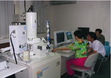
The field emission scanning electron microscope (SEM) uses negative pressure applied to a metal tip to extract electrons from the tip and generate a very small electron beam. Operating in ultra-high vacuum (-10-10 torr), it can produce high-quality resolution images. With the development of science and technology, nanoscience and nanotechnology have become the mainstay of national high-tech development. They can meet the requirements of smaller and finer components, control the material composition, interface structure, and manipulate them within 1-100 nanometers. Observing the resulting changes in physical, chemical, and biological properties can be applied to industry. The FE-SEM provides the most important tool for measuring and manipulating these nanostructures.
Equipment Description
Model:JEOL JSM-6330TF
| Resolution | 1.5nm(15kv), 5.0nm(1.0kv) |
| Acceleration | 0.5kv to 30kv (100v steps) |
| Magnification | x10 to x500,000 |
| GUN | Thermal field effect type In-Lens Thermal |
| Image mode |
SEI(Secondary Electron Image) BEI TOPO/COMP(Back Electronic Image) |
| Maximum allowable sample | 25mm diameter x 10mm height |
| Live image display | 1280x1024 pixels |
| Specimen stage |
Eccentric X=70mm, Y=50mm, Z=3mm~41mm R=360°,T=-5~60° |
- CL (Cathodoluminescence System) Cathodoluminescence Detection System
Service Items
- SEI(Scanning Electron Image)material surface structure observation, broken surface observation, thin film coating observation
- BEI(Backscatter Electron Image)backscattered electron image observation
- Energy Dispersive Spectrometer can be used for qualitative, semi-quantitative analysis of micro-region components, linescan and mapping
Sampling Precautions
- For SEI, BEI and CL parts: the size and diameter of the specimens should be within 25mm, and the height should not exceed 10mm. Please pre-process the test piece by yourself.
- The surface of the sample needs to be conductive, and the sample with a non-conductive surface needs to be carbon-plated or gold-plated, please handle it yourself first. If there is no prior processing, there is also on-site, but an additional cash fee is required (NT$200 per time)
- Please bring your own CD to access the files, it is forbidden to access files with flash drives.
- Cancellation notice is required 2 days in advance, otherwise a penalty may be imposed. The basic usage fee will still be charged, and the appointment will be given to the next person on the waiting list.
- Toxic, corrosive, volatile, magnetic, or low melting point materials are prohibited.
- Please contact the technician by phone in advance for the preparation method of nano powder.
- Please fill out the 'Polymer Application Form' for polymer materials. After review and approval, you may proceed to make a reservation.
Charges
|
Project |
Non-project |
Training |
Certified |
Fee Description |
|||
|
Self-operated |
Entrust |
Self-operated |
Entrust |
Fee |
Time |
||
|
200 |
300 |
1500 |
300/HR |
6 |
1000 |
Hourly billing A session is 3 hours |
|
Less than 1 hour will be charged as 1 hour
Additional use:
- An additional NT$50/point is charged for point analysis of the EDS system
- An additional NT$100/point is charged for surface and line analysis
- Additional NT$150 per hour for CL system
Contact Detail