
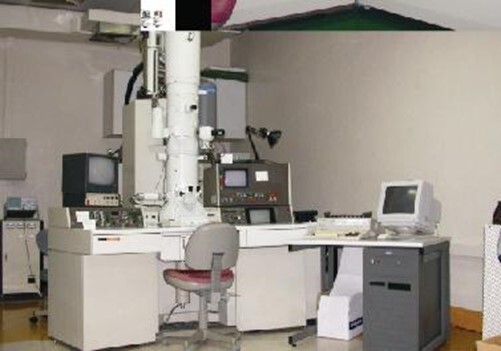
JEOL 3010 Analytical Scanning Transmission Electron Microscope
This instrument is suitable for solid nanomaterials, semiconductor electronic materials, ceramic mineral materials, metal materials, polymer materials, etc. With 300KV high-energy electrons penetrating the test piece, the shape of the object can be observed, the size can be measured, and the microstructure, defects and crystal structure inside the material can be analyzed. It can simultaneously provide HR high-resolution analysis, EDS micro-area chemical composition analysis, Microdiffraction micro-beam diffraction analysis, high-angle multi-directional diffraction analysis and high-quality bright and dark field images. With dual functions of analytical and high-resolution microscopy, it is an indispensable tool for studying and analyzing materials in the microscopic world.
Equipment Description
- Model:JEOL JEM-3010 Analytical Scanning Transmission Electron Microscope
- Specifications:
- Accelerating Voltage:0~300KV
- Magnification:50~1,200,000X
- Resolution:Point : 0.21nm; Lattice : 0.14nm
- pot size : 1.5~200nm
- CBED : convergent angle : 1.5~20mrad
- Double inclined test piece holder:X axis ± 40°;Y axis ± 30°
- Appendix:
- X-ray component analysis system(EDS)
- Model: EDS X-MAX80T for 300kv TEM
- SDD internal integrated FET
- Sensor size: 80mm2 active area
- Detector Window: SATW Ultra thin polymer window
- Model: EDS X-MAX80T for 300kv TEM
- X-ray component analysis system(EDS)
- Function and usage
- With scanning and penetrating functions, it can be used for observation and analysis of microstructure, crystal structure and defects of various solid materials
- Can be used for microbeam diffraction analysis (Microdiffraction), including CBED analysis (Convergent Beam Electron Diffraction), and identifying the microstructure of crystalline materials
- Also used for high-resolution (HREM) to enhance the signal and magnify the image to analyze the microstructure of crystalline materials
- Qualitative and quantitative full-energy spectrum analysis of chemical elements:5B~92U
Service Items
- Observation analysis and microbeam diffraction analysis
- Elemental analysis and high-resolution imaging analysis
Charges
- Project:The fee for filament usage is NT$400 per hour, calculated in 3-hour blocks
- Non-project:The fee for filament usage is NT$1500 per hour, calculated in 3-hour blocks
- Extra $10 per photo
- An additional $200 per hour charged for using EDS and HR analysis
Preparation of specimens
- Size:3mm diameter with thinned perforators
- Samples that will decompose or release gas under electron beam irradiation and ferromagnetic materials will not be accepted
Contact Detail