
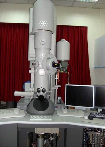
FEG-TEM Tecnai F20 G2 Field Emission Gun Transmission Electron Microscope
The instrument (Tecnai F20 G2) can be used to analyze solid-state, nano, semiconductor, mineral, metallic and biomedical materials. Field-emitted high energy electrons of 200 kV can be applied in transmission or scanning mode to analyze the microstructures including morphology, size, defect and crystalline structure. Advanced functions are available such as atomic number contrast image, high resolution image, convergent beam electron diffraction (CBED), micro-diffraction, micro-area energy dispersion spectroscopy (EDS) analyses of chemical composition, elemental mapping and elemental line profile, and electron energy loss spectroscopy (EELS) analyses of light elements chemical composition, elemental mapping and atomic bond configuration. The instrument has a high-angle double-tilt stage for multiple-angle electron diffraction analysis with high quality bright and dark field images. It is an advanced instrument indispensable in the analysis of micro and nano structures of materials.
Equipment Description
- Model:Tecnai F20 G2 MAT S-TWIN Field Emission Gun Transmission Electron Microscope
- Specifications:
- Accelerating Voltage:20~200KV
- Magnification:X 25~1.03M
- Resolution:Point:0.23nm;Line Resoltion:0.1nm;Information Resoltion:0.15nm
- Spot size:TEM:8.5~350nm;Microprobe:1~25nm;Nanoprobe:0.3~5nm
- CBED:convergent angle:1.5~20mrad
- Double inclined test piece holder:X axis ± 40°;Y axis ± 30°
- STEM equipped with HAADF Detector and BF/DF Detector
- Gatan CCD(2K×2K)
- Appendix:
- EDS Analysis X-ray Energy Dispersion Analyzer
Oxford AZtec Energy Advanced (plus IE350) with X-MaxN 80
- Si drift detector (SDD) (LN2 free), 80mm2
- Resolution:≦129ev
- Gatan Image Filter / Electron Energy Loss Spectroscopy equipped with Windows operating system: Auto PEELS software;CCD(2K×2K)
- STEM scanning imaging control system equipped with HAADF Detector
- Multiscan CCD Camera Charge Coupled Device Imaging Accessory
Gatan Charge Coupled Device Camera(2K×2K)
- Function and usage
- With scanning and penetrating functions, it can be used for observation and analysis of microstructure, crystal structure and defects of various solid materials
- Also used for high-resolution (HREM) to enhance the signal and magnify the image to analyze the microstructure of crystalline materials
- Can be used for microbeam diffraction analysis (Microdiffraction), including CBED analysis (Convergent Beam Electron Diffraction), and identifying the microstructure of crystalline materials
- Qualitative and quantitative full-energy spectrum analysis of chemical elements (EDS): 5B~92U
- Can analyze chemical element distribution, EDS Mapping and Line Profile analysis
- Used for electron energy loss spectroscopy (EELS) to analyze chemical element composition (light elements) and atomic bonding configuration
Service Items
(1) Microscopic observation analysis (2) High-resolution imaging analysis (3) Microbeam diffraction analysis
(4) Scanning HAADF analysis (5) Electron energy loss spectrum analysis
(6) Chemical composition EDS Point, Line Profile and Mapping analysis (7) CCD photo
Charges
- NT$600 per hour, calculated in 3-hour blocks. Overtime will be charged once per hour.
(1) HR Analysis (2) NBD/CBD Analysis (3) STEM Analysis(HAADF) (4) EDS Analysis (Point,Line scan,Mapping):First four NT$100 per hour
(5) EELS/GIF Analysis:NT$200 per hour
- Project:
delegated $600/per hour, details charged as above
self-operation $300/per hour, details will be charged half
- Non-Project:delegated $2000/per hour, details will be charged triple
Preparation of specimens
- In the shape of a disc with a diameter of 3 mm, and must be a solid material that has been thinned, perforated and conductive
- Samples that will decompose or release gas under electron beam irradiation, polymer materials, magnetic powders and ferromagnetic materials will not be accepted.
Contact Detail