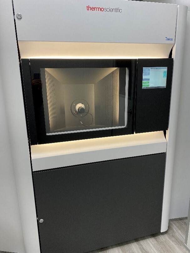
Talos F200E Field Emission Scanning Transmission Electron Microscope
High-resolution field emission scanning transmission electron microscope (Talos F200X G2) is suitable for metals, semiconductor electronics, ceramic minerals, biomedical catalysts, polymers, metal organic framework materials, and electron beam-sensitive materials, etc. Field emission of 80-200KV electrons with different energies penetrates the specimen and has the function of penetration and scanning. It can observe the morphology of the object, dimension measurement, particles-size calculation, the microstructure and defects of the material. In addition, it can simultaneously provide high-resolution analysis, micro/nano-beam diffraction analysis, TEM-EDS/STEM-EDS atomic-level chemical composition analysis, chemical element mapping and line profile analysis, and 3D EDS Tomography analysis. And it can be used for high-angle multi-directional diffraction analysis and high-quality bright and dark field images. These functions combine the multiple functions of atomic-level analysis and high-resolution microscopy.
Instrument Description
- Model: FEI (Thermo Fisher Scientific), Talos F200X G2 Field Emission Scanning Transmission Electron Microscope
Main Specifications
-
Accelerating voltage: 20~200KV
-
Magnification: TEM magnification range 25x-1.50Mx, STEM magnification range 50x-230Mx
-
Resolution: TEM information limit ≤ 0.12 nm, TEM point resolution ≤ 0.25 nm, STEM high angle annular dark field (HAADF) resolution ≤0.16 nm
-
Maximum tilt angle with double tilt holder: ±30˚
-
EDS system: Bruker, Symmetrical design 2 Dual-X 6T 100RT
-
Fast EDS mapping: pixel dwell time down to 10 µs
-
EDS Effective solid angle: 1.65 srad
-
Camera: Low-distortion Ceta 4k x 4k, Ceta Speed Enhancement (40 fps)
-
Camera length: 12-5700 mm
-
Maximum diffraction angle: ±24°
-
STEM detector: BF, DF2, DF4, HAADF
Function and Application
- TEM has the functions of penetrating and scanning, and can analyze the microstructure and crystal structure of various solid materials and observe micro-defects.
- High-resolution electron microscope (HRTEM/HRSTEM) image can be used to analyze the microstructure of crystalline materials
- With Nano-Beam Diffraction (NBD) and Convergent Beam Electron Diffraction (CBED) analysis functions
- It has qualitative and quantitative full-energy spectrum analysis of chemical element composition, EDS mapping and EDS line profile analysis in TEM/STEM mode.
- EDS tomography reconstructs a three‐dimensional (3D) elemental map.
- A new low-beam dose TEM techniques, Differential Image Contrast Imaging (DPC/iDPC-STEM) can effectively image beam sensitive materials.
- Turnkey analytical services and consulting.
Service Items
-
Microscopic observation and analysis: bright-field and dark-field images
- High-resolution imaging analysis (HRTEM/HRSTEM).
- Diffraction analysis, convergent beam electron diffraction and micro-beam diffraction analysis.
- EDS is used under TEM/STEM mode to acquire images and spectral signals under different detectors, and can deal with EDS point/line/surface scanning analysis of chemical composition.
- Among the new low beam dose TEM techniques, Differential Image Contrast Imaging (DPC/iDPC-STEM) can efficiently image electron beam sensitive materials.
- 3D tomography image and chemical composition analysis.
- Data and pictures are obtained by burning DVD discs.
Charges
-
With a National Science and Technology Council (NSTC) program: each session is calculated as 3 hours, and the filament usage time is charged NT$ 600 per hour.
- Without a National Science and Technology Council (NSTC) program: each session is calculated as 3 hours, and the filament usage time is charged NT$ 2500 per hour.
- (1) High-resolution imaging analysis is charged NT$150 per hour, (2) NBD/CBD analysis is charged NT$100 per hour.
- EDS (point/line/map) analysis is charged NT$200 per hour.
- STEM (BF/DF/HAADF) analysis and HRSTEM analysis is charged NT$300 per hour.
- Differential phase contrast STEM analysis is charged NT$300 per hour.
- High-resolution atomic image EDS (point/line/map) analysis is charged NT$500 per hour.
- For the turnkey analysis service, in addition to the instrument usage fee, an additional NT$300 per hour will be charged.
- Notice 7 days in advance to cancel the booking, otherwise a basic fee of NT$900 will be charged.
Specimen preparation
- Specimen dimension: the specimen is mainly composed of (1) thinned perforated foil, (2) carried on a carbon (lacey) TEM support films copper grid with a diameter of 3mm, and (3) an Omniprobe Lift-Out.
- If the powder sample contains suspension, it is necessary to dry the specimen with vacuum.
- Polymer and organic solution sample are unavailable service. If you have analysis needs, please contact Mr. Lin Xiancan, the technician in charge of the center's polymer dedicated TEM (JEOL JEM-2100).
- It is strictly forbidden to serve the ferromagnetic materials, and the material with decompose or release gas under electron beam. For magnetic test pieces, please contact the technical personnel in charge or Dr. Huang (07-5252000#4075) of our center for consultation.
- .If you have any questions regarding the pretreatment of test samples, please contact Dr. Hui-Jun Huang at our center (Tel: 07-5252000 ext. 4075) or via e-mail at m9036601@student.nsysu.edu.tw
Contact Us